TSMC CoWoP Explained: What You Gain (and Lose) Dropping the ABF Substrate
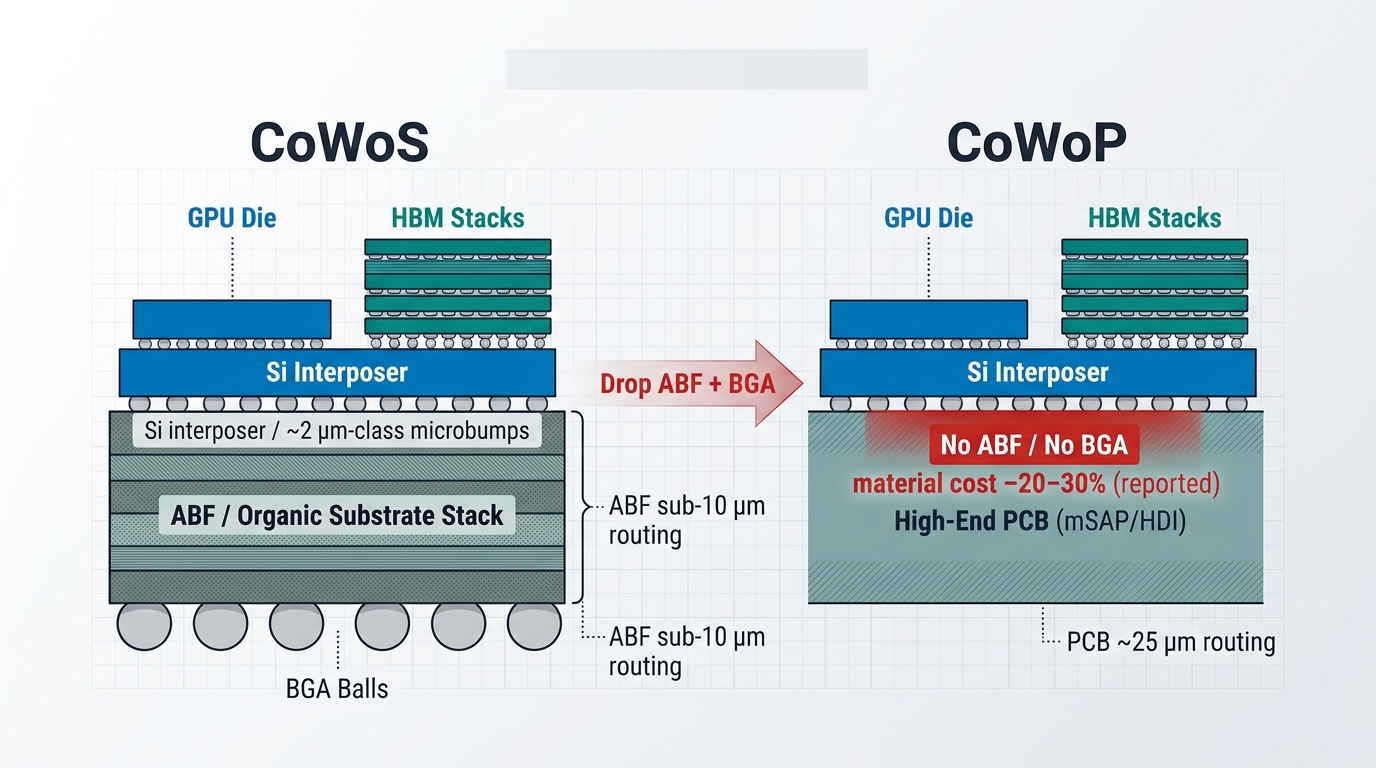
Bottom line: In today's CoWoS stack, the silicon interposer is expensive — but the ABF/BT package substrate plus BGA underneath is often where capacity and cost really bite. The supply-chain idea labeled CoWoP (Chip-on-Wafer-on-PCB) is blunt: keep the interposer for micron-class GPU↔HBM links, then land the whole Chip-on-Wafer stack on a high-end PCB and skip the classic package substrate and balls. Material savings, a shorter path, a simpler bill of materials — attractive on a slide. Coarser board pitch, warpage and yield are the other half of the story.
What happened
- Definition (industry-analysis language, not a formal TSMC product launch): CoWoP keeps the silicon interposer for GPU↔HBM fine pitch and replaces the ABF/BT substrate + BGA with an mSAP/HDI-class PCB (DigiTimes, CTEE and related supply-chain reporting).
- Claimed benefits in that reporting: roughly 20–30% lower packaging-material cost by dropping ABF+BGA; electrical path shortened by about 40% in one DigiTimes note; simpler supply chain; thermal path that no longer crosses ABF; PCB capacity and cycle-time advantages versus constrained ABF lines.
- Industrial pressure: at OCP APAC 2026, TSMC advanced-packaging head Jun He said 5.5x-reticle CoWoS is in volume at ~98–99% yield and called out ABF substrates and memory as bottlenecks — the backdrop that makes "skip the substrate" ideas interesting (third-party recap).
- Market rumor: NVIDIA may dual-path CoWoS + CoWoP for Rubin GR150 (supply-chain chatter around Oct 2026). JPM, Morgan Stanley, Ming-Chi Kuo and others sound skeptical on mid-term volume. TSMC's own clearer public narrative remains CoPoS panel-level packaging (pilot narrative ~2026, volume ~2028). Relative to CoPoS, CoWoP is still an early concept.
- Fan-page / market synthesis (not audited filings): silicon interposer around US$15k, 14-layer ABF yield stress, ~+20% price rumors, Rubin lead times near 52 weeks. October earnings-call commentary also described a "very large gap" in advanced-packaging demand.
The value of the CoWoS family still sits in micron-class microbumps and fine routing on the silicon interposer between GPU and HBM. CoWoP does not claim to rewrite that tier. It rewrites everything under the interposer: instead of a high-density ABF substrate and a BGA down to the system board, the CoW stack lands on a producible high-end PCB. The supply-chain bet is that ABF capacity and lead time are the choke points PCB shops can relieve, while the material line item sheds an expensive substrate and a ball layer.
Point 2: 20–30% material savings ≠ 20–30% module costThe reporting language is packaging-material cost down about 20–30%. Author illustration: if ABF+BGA already take a meaningful slice of the CoWoS materials BOM, landing in that band after removing them is plausible. The same reporting notes PCB process fees can run about 2× a normal board, before warpage compensation, test and rework. So "materials −20–30%" is not "finished module −20–30%." Without a public BOM split, treat the range as a supply-chain claim, not an audited figure.
Point 3: The pitch tax — board-side I/O roughly ≥2.5× coarserABF substrates can route at sub-10 µm line/space. High-end PCB mSAP is commonly about 25/25 µm. Author illustration: 25 ÷ 10 = 2.5, so board-side pitch is roughly ≥2.5× coarser (illustration, not a lab measurement). Fine pitch on the interposer must therefore coarsen through redistribution or fewer direct board I/Os — SI, power-plane splits and escape routing all get redesigned. DigiTimes' ~40% shorter-path claim is directionally sensible (one fewer substrate and BGA height), but it is reported, not measured here.
Point 4: Warpage, CTE and yield are the real invoiceSilicon interposer CTE sits near silicon; organic ABF and PCB CTE sit much higher. Bonding a large CoW stack straight to PCB does not make thermo-mechanical stress vanish — it moves which layer absorbs it and which underfill or stiffener has to cope. A few points of yield loss, especially after expensive HBM attach, quickly erase material savings. That is why analysts stay cautious about CoWoP eating Rubin-era volume: a capacity hedge or demo path is one thing; displacing mainstream CoWoS is another. The PLC fan page framed the same substrate-pressure angle here: FB post on CoWoP and substrate pressure.
Open questions
- TSMC has not listed CoWoP as a formal volume platform alongside CoWoS/CoPoS; this article follows DigiTimes/CTEE-class supply-chain analysis.
- "Materials −20–30%," "path −40%" and "~2× PCB process fee" are reporting claims without a public BOM or bench measurement.
- NVIDIA Rubin dual-path, 52-week leads and ~US$15k interposer figures are fan-page / market synthesis, not filings or datasheets.
- CoPoS (panel, ~2028 volume narrative) also targets substrate/capacity pressure but is a different process and timeline — do not conflate the two.
Related videos
 You Think TSMC's CoWoS is Just One Technology? (S, R, & L Explained)
 SoIC Stacking: Interconnect One Step Closer Than CoWoS
Is CoWoP mainly a CoWoS capacity hedge, or can it take real Rubin-era volume? Tell me in the comments.
Published on The Automation Core. Videos by @TheEngineeringCore-v. Join the discussion on the PLC Facebook page.

