
Bottom line: TSMC refreshed its SoIC roadmap at this year’s Technology Symposium, so it is a good time to revisit how 3D chip stacking actually works. SoIC-X uses bumpless hybrid bonding to chase density and energy per bit; SoIC-P keeps micro-bumps to chase cost. The deciding variable between them is bond pitch.
What happened
- Roadmap: TSMC says 9 µm-pitch N7-on-N7 SoIC has been in production since 2023 and the 6 µm version since 2025. N2-on-N2 at 6 µm is planned for 2028, and A14-on-A14 at 4.5 µm for 2029.
- A14 SoIC: TSMC’s press release says A14-to-A14 SoIC gives 1.8× the die-to-die I/O density of N2-on-N2.
- Capacity: Supply-chain reports cited by TrendForce put 2026 SoIC capacity at roughly 10,000–15,000 wafers per month, mostly at AP6 in Zhunan, with capex estimated at $6.8–7.0B per 10,000 wafers, far above CoWoS.
- But priorities shift: DIGITIMES reported in January that phases P2 and P3 at the AP7 site in Chiayi, originally planned for SoIC, were switched to CoWoS because the CoWoS shortage is more urgent.
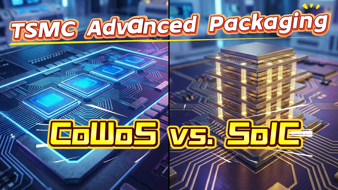
Quick way to tell them apart: SoIC-X bonds two dies copper-to-copper with no solder in between. SoIC-P still has a row of tiny solder bumps. One makes two floors of the same building; the other connects two buildings with many small skybridges.
Engineering point 1: what separates SoIC-X from SoIC-P
SoIC-X is bumpless stacking. Both die surfaces are planarized so copper pads sit flush with the dielectric; after alignment the dielectric bonds first and an anneal makes the copper pads diffuse into each other. Signals then drop through thin TSVs. It is offered as chip-on-wafer and also as wafer-on-wafer, which suits equal-size dies on high-yield nodes. SoIC-P keeps micro-bumps. When TSMC introduced it in 2023 it quoted 18–25 µm pitch for cost-sensitive mobile, IoT and client parts, with a roadmap from 25 µm face-to-back toward 16 µm face-to-face. In short, X is for performance and P is for price.
Engineering point 2: why a few microns of pitch change everything
Pads sit on a grid, so pads per mm² scale roughly with 1/pitch². Using an ideal square grid (illustrative, not usable I/O): 25 µm gives about 1,600 per mm², 16 µm about 3,900, 9 µm about 12,300, 6 µm about 27,800 and 4.5 µm about 49,400. Going from 25 µm micro-bumps to 6 µm hybrid bonds is about 17× in theoretical density. More pads let you replace a few fast, long, power-hungry SerDes-style links with many slow, short, wide ones, which cuts energy per bit. AMD’s MI300 packaging paper claims hybrid bonding delivers more than 15× interconnect density and more than 3× interconnect energy efficiency versus micro-bumps. Broadcom has cited about 1,500 signals/mm² for face-to-back versus about 14,000 signals/mm² for face-to-face stacking.
Engineering point 3: yield, heat and KGD are the real gatekeepers
Hybrid bonding has no solder to absorb errors, so surfaces must be extremely flat and clean: a single particle can void a region, and alignment accuracy has to shrink along with pitch. Next comes compound yield: if either die in a stack is bad, the whole stack is scrap, so chip-on-wafer flows stack only known-good dies (KGD). But fine-pitch pads are hard to probe, so the test strategy has to be designed up front. Then there is heat: the top die’s heat must pass through the bottom die, and logic-on-logic hot spots warm each other. That is one reason early AMD 3D V-Cache parts placed cache over the CCD and capped clocks. All of this shows up in cost, which is why analysts put SoIC capex per wafer far above CoWoS.
Engineering point 4: SoIC plus CoWoS or InFO makes a full 3D IC
SoIC only handles the vertical stack. From the outside the stacked die looks like an ordinary SoC, which then goes into CoWoS (2.5D interposer with HBM alongside) or InFO (fan-out packaging common in phones). AMD’s MI300 is the reference design: compute dies hybrid-bonded onto I/O dies, then placed on a CoWoS interposer with HBM, a stack AMD calls 3.5D. Looking ahead, supply-chain reports say NVIDIA’s 2028 Feynman generation will use far more SoIC, and TrendForce, citing reports, says Apple’s M5 Pro and M5 Max adopt TSMC SoIC-family packaging. HBM stacking itself is a separate story we covered on October 21.
Open questions
- The pads-per-mm² figures are ideal-grid illustrations; usable signal counts are much lower after power, ground and redundant pads.
- A 2024 roadmap slide showed 3 µm by 2027, while TSMC’s 2026 official wording is 4.5 µm A14-on-A14 in 2029. The framings differ; this post follows the 2026 official data.
- 2026 capacity, capex per 10,000 wafers and NVIDIA/Apple adoption come from supply-chain and media reports, not TSMC disclosures.
Watch the video
Main video: Beyond CoWoS: Why TSMC's SoIC is the Real Future of Chips
▶ Watch on The Engineering Core
Related: You Think TSMC's CoWoS is Just One Technology? (S, R, & L Explained) and The End of Copper: How Silicon Photonics is Saving AI (TSMC’s COUPE optical engine is itself SoIC-stacked).
Will next-gen AI chips go all-in on SoIC-X hybrid bonding, or will cost keep SoIC-P and CoWoS around longer? Let me know in the comments.
Published on The Automation Core | Video: The Engineering Core YouTube channel (@TheEngineeringCore-v)

